| CPC H01L 24/17 (2013.01) [H01L 23/49816 (2013.01); H01L 23/49827 (2013.01); H01L 23/49838 (2013.01); H01L 23/49894 (2013.01); H01L 23/528 (2013.01); H01L 24/02 (2013.01); H01L 24/09 (2013.01); H01L 24/14 (2013.01); H01L 24/16 (2013.01); H01L 24/33 (2013.01); H01L 24/81 (2013.01); H01L 25/0657 (2013.01); H01L 25/105 (2013.01); H01L 29/66 (2013.01); H05K 1/111 (2013.01); H01L 23/3192 (2013.01); H01L 24/05 (2013.01); H01L 24/13 (2013.01); H01L 2224/0235 (2013.01); H01L 2224/02375 (2013.01); H01L 2224/0401 (2013.01); H01L 2224/05073 (2013.01); H01L 2224/05166 (2013.01); H01L 2224/05548 (2013.01); H01L 2224/05572 (2013.01); H01L 2224/05647 (2013.01); H01L 2224/1308 (2013.01); H01L 2224/13022 (2013.01); H01L 2224/13082 (2013.01); H01L 2224/13111 (2013.01); H01L 2224/13144 (2013.01); H01L 2224/13147 (2013.01); H01L 2224/13155 (2013.01); H01L 2224/13164 (2013.01); H01L 2224/14133 (2013.01); H01L 2224/16013 (2013.01); H01L 2224/16145 (2013.01); H01L 2224/16148 (2013.01); H01L 2224/16227 (2013.01); H01L 2224/16238 (2013.01); H01L 2224/3003 (2013.01); H01L 2224/81191 (2013.01); H01L 2224/81192 (2013.01); H01L 2224/81385 (2013.01); H01L 2224/81815 (2013.01); H01L 2225/06513 (2013.01); H01L 2225/1047 (2013.01); H01L 2225/1058 (2013.01); H01L 2924/3512 (2013.01); H01L 2924/35121 (2013.01); H01L 2924/3841 (2013.01); H05K 2201/09727 (2013.01); H05K 2201/10674 (2013.01); Y02P 70/50 (2015.11)] | 20 Claims |
|
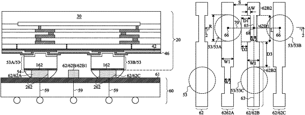
1. A method comprising:
forming a first package component comprising:
a first metal trace comprising:
a first portion having a first width;
second portions connecting to opposing ends of the first portion, wherein the second portions have second widths greater than the first width; and
bonding a second package component to the first package component, wherein a first solder region joins the second package component to a second metal trace of the first package component, and a center of the first solder region is aligned to a straight line that extends from a middle point of the first portion toward the second metal trace, and wherein the straight line is perpendicular to a lengthwise direction of the first metal trace, and wherein after the bonding, the first portion of the first metal trace is free from any solder region that is directly on and in physical contact with both of a top surface and sidewall surfaces of the first portion of the first metal trace.
|