| CPC H01L 24/05 (2013.01) [H01L 24/03 (2013.01); H01L 24/45 (2013.01); H01L 24/85 (2013.01); H01L 2224/05017 (2013.01)] | 9 Claims |
|
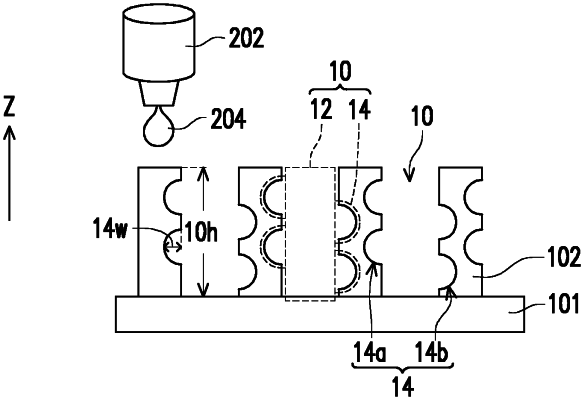
1. A semiconductor device, comprising:
a passivation layer disposed on a substrate; and
a connector embedded in the passivation layer, wherein an interface of the connector in contact with the passivation layer is uneven, wherein the connector comprises:
a body portion having opposite sidewalls perpendicular to the substrate;
and a plurality of protrusion portions protruding outward from the opposite sidewalls of the body portion, wherein the plurality of protrusion portions are staggered with each other in a Z direction.
|