| CPC H01L 24/02 (2013.01) [H01L 23/13 (2013.01); H01L 23/49811 (2013.01); H01L 23/49827 (2013.01); H01L 24/13 (2013.01); H01L 24/17 (2013.01); H01L 24/32 (2013.01); H01L 25/105 (2013.01); H01L 25/18 (2013.01); H01L 23/3128 (2013.01); H01L 23/49816 (2013.01); H01L 23/49822 (2013.01); H01L 23/49838 (2013.01); H01L 24/05 (2013.01); H01L 24/16 (2013.01); H01L 24/29 (2013.01); H01L 2224/02331 (2013.01); H01L 2224/02373 (2013.01); H01L 2224/02375 (2013.01); H01L 2224/02379 (2013.01); H01L 2224/02381 (2013.01); H01L 2224/0401 (2013.01); H01L 2224/13022 (2013.01); H01L 2224/13024 (2013.01); H01L 2224/13101 (2013.01); H01L 2224/16225 (2013.01); H01L 2224/16235 (2013.01); H01L 2224/16237 (2013.01); H01L 2224/2919 (2013.01); H01L 2224/32014 (2013.01); H01L 2224/32058 (2013.01); H01L 2224/32225 (2013.01); H01L 2224/73204 (2013.01); H01L 2225/1011 (2013.01); H01L 2924/15311 (2013.01); H01L 2924/15331 (2013.01)] | 18 Claims |
|
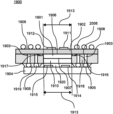
1. An electronic device, comprising:
a redistribution structure, the redistribution structure having a front surface and a back surface, the redistribution structure comprising a set of metal layers and a set of insulating layers, at least a middle metal layer of the set of metal layers comprising a plurality of holes, at least a subset of the plurality of holes forming a mesh type area, at least a width of one of the plurality of holes being greater than a width of an inner line of the mesh type area;
a processor die, the processor die having a front side and a back side, the front side of the processor die being connected to the front surface of the redistribution structure, the processor die comprising a passivation layer on the front side, the electronic device comprising an insulating layer on the passivation layer of the processor die;
a molding material;
a set of conductive posts, the set of conductive posts being placed beside the processor die, the molding material surrounding the set of conductive posts, the set of conductive posts being connected to the front surface of the redistribution structure;
a first set of solder bumps, the first set of solder bumps being connected to the set of conductive posts;
a second set of solder bumps, the second set of solder bumps being connected to the back surface of the redistribution structure; and
an underfill material, the underfill material surrounding the first set of solder bumps;
wherein a recess is formed between the redistribution structure and the processor die, there is a horizontal shift between a die edge of the processor die and an outer edge of the insulating layer, and the recess is filled with the molding material.
|