| CPC H01L 23/66 (2013.01) [G01S 13/08 (2013.01); H01L 23/49816 (2013.01); H01L 24/16 (2013.01); H01Q 1/2283 (2013.01); G01S 13/931 (2013.01); H01L 2223/6622 (2013.01); H01L 2223/6633 (2013.01); H01L 2223/6677 (2013.01); H01L 2224/16225 (2013.01)] | 20 Claims |
|
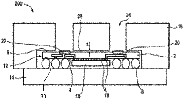
1. A semiconductor device, comprising:
a substrate having a first surface and a second surface opposite the first surface;
at least one connection element arranged on the first surface of the substrate to electrically and mechanically connect the substrate to a printed circuit board;
a radar semiconductor chip arranged on the first surface of the substrate; and
at least one of:
a waveguiding transformer element comprising a first surface and a second surface, wherein the first surface of the waveguiding transformer element resides above the first surface of the substrate, and wherein the second surface of the waveguiding transformer element is embedded into the substrate,
a radar antenna at least partially embedded into the substrate, or
a waveguide transition element embedded into the substrate, wherein the first surface of the substrate exposes a first end of the waveguiding transformer element, wherein the second surface of the substrate exposes a second end of the waveguiding transformer element.
|