| CPC H01L 23/645 (2013.01) [H01L 21/4857 (2013.01); H01L 23/145 (2013.01); H01L 23/49822 (2013.01); H01L 23/49838 (2013.01); H01L 24/16 (2013.01); H01L 28/10 (2013.01); H01L 28/40 (2013.01); H03H 7/0115 (2013.01); H01L 2224/16227 (2013.01); H01L 2924/19041 (2013.01); H01L 2924/19042 (2013.01); H01L 2924/19103 (2013.01)] | 20 Claims |
|
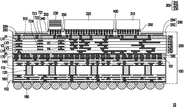
1. A structure, comprising:
a first via and a first conductive line embedded in a first dielectric layer and spaced apart from each other by the first dielectric layer;
a first metal pattern disposed on the first via and embedded in a second dielectric layer;
a first conductive via disposed on the first conductive line and embedded in the second dielectric layer, wherein the first metal pattern and the first conductive via are spaced apart from each other and are located on a first horizontal level, and the first metal pattern has an open ring shape;
a second via disposed on the first metal pattern and embedded in a third dielectric layer;
a second conductive line disposed on the second conductive via and embedded in the third dielectric layer;
a second metal pattern disposed on the second via and embedded in a fourth dielectric layer; and
a second conductive via disposed on the second conductive line and embedded in the fourth dielectric layer, wherein the second metal pattern and the second conductive via are spaced apart from each other and are located on a second horizontal level, the second metal pattern has an open ring shape, and the first metal pattern vertically partially overlaps the second metal pattern,
wherein the first via, the first metal pattern, the second via and the second metal pattern are electrically connected, and an inductor structure including the first via, the first metal pattern, the second via and the second metal pattern extends from the first dielectric layer to the fourth dielectric layer.
|