| CPC H01L 23/562 (2013.01) [H01L 21/4825 (2013.01); H01L 21/565 (2013.01); H01L 23/3107 (2013.01); H01L 23/4952 (2013.01); H01L 23/49513 (2013.01); H01L 23/49562 (2013.01); H01L 23/49575 (2013.01)] | 30 Claims |

|
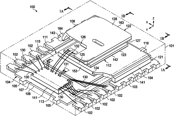
1. A packaged electronic device, comprising:
a semiconductor die having a first side, an opposite second side and a terminal exposed along the second side of the semiconductor die;
a conductive plate having a first side, an opposite second side and an indent, the indent extends into the first side, the conductive plate electrically coupled to a lead;
a solder structure that extends between the second side of the semiconductor die and the first side of the conductive plate to electrically couple the conductive plate to the terminal exposed along the second side of the semiconductor die, the solder structure extends into the indent; and
a package structure that encloses the semiconductor die, the conductive plate and a portion of the lead, the package structure exposes a portion of the lead.
|
|
8. A method of manufacturing a packaged electronic device, the method comprising:
forming an indent in a side of a conductive plate;
depositing solder on a side of a semiconductor die;
engaging the side of the conductive plate with the solder to form a solder structure that extends between the side of the semiconductor die and the side of the conductive plate, the solder structure extends into the indent;
heating the solder to electrically couple the conductive plate to a terminal exposed along the side of the semiconductor die; and
forming a package structure that encloses the semiconductor die and the conductive plate.
|