| CPC H01L 23/5226 (2013.01) [H01L 21/76807 (2013.01); H01L 29/41791 (2013.01); H01L 21/76877 (2013.01); H01L 23/53257 (2013.01); H01L 29/45 (2013.01); H01L 29/785 (2013.01); H01L 2221/1036 (2013.01)] | 19 Claims |
|
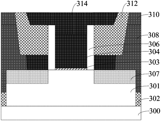
1. A semiconductor structure, comprising:
a substrate;
a gate structure on the substrate, wherein the gate structure extends along a first direction, the gate structure includes a gate dielectric layer, a gate electrode layer on the gate dielectric layer, a protective layer on the gate electrode layer, and sidewall spacers at sides of the gate electrode layer and the protective layer, and the protective layer and the sidewall spacers are made of a first material;
source/drain doped layers in the substrate at sides of the gate structure;
a first conductive structure on the source/drain doped layers, wherein an opening is formed on the gate structure and the first conductive structure, wherein the opening extends along a second direction different from the first direction;
a second conductive structure in the opening, wherein the second conductive structure is insulated from the first conductive structure and in contact with the gate structures; and
an insulating layer in the opening, wherein the insulating layer is disposed between the first conductive structure and the second conductive structure, and the insulating layer is made of a second material different from the first material.
|