| CPC H01L 23/49827 (2013.01) [H01L 21/56 (2013.01); H01L 21/76816 (2013.01); H01L 21/76871 (2013.01); H01L 23/3107 (2013.01); H01L 23/481 (2013.01); H01L 23/66 (2013.01); H01L 24/09 (2013.01); H01Q 1/2283 (2013.01); H01Q 9/0407 (2013.01); H01Q 9/285 (2013.01); H01L 2223/6677 (2013.01); H01L 2224/02372 (2013.01)] | 20 Claims |
|
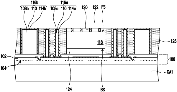
7. A manufacturing method of a semiconductor package, comprising:
forming an insulating layer over a carrier;
patterning the insulating layer to form a first insulating core and a second insulating core;
forming a first seed layer and a first conductive layer on a top surface and a sidewall of the first insulating core;
forming a second seed layer and a second conductive layer on a top surface and a sidewall of the second insulating core;
attaching a semiconductor die onto the carrier, wherein a through via structure comprising the first insulating core, the first seed layer and the first conductive layer as well as a dipole structure comprising the second insulating core, the second seed layer and the second conductive layer are located aside the semiconductor die;
laterally encapsulating the through via structure, the dipole structure and the semiconductor die with an encapsulant; and
removing the carrier.
|