| CPC H01L 23/3672 (2013.01) [H01L 21/4882 (2013.01)] | 15 Claims |
|
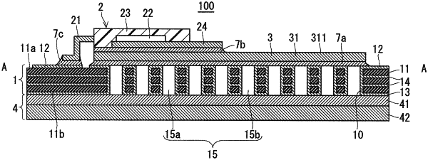
1. A semiconductor device comprising:
a printed circuit board;
a heat diffusion part bonded to a first main face of the printed circuit board with a first bonding material;
an electronic component including a heat radiator plate bonded to the heat diffusion part with a second bonding material; and
a heat radiation part disposed directly on a second main face of the printed circuit board,
wherein the printed circuit board includes:
an insulation layer;
first and second conductor layers disposed respectively on first and second main faces of the insulation layer;
a plurality of heat radiation vias penetrating from the first conductor layer to the second conductor layer on the insulation layer; and
a conductor film covering inner walls of the plurality of heat radiation vias,
the plurality of heat radiation vias is provided at positions overlapping the heat diffusion part and the electronic component in plan view viewed from the first main face of the printed circuit board, and
the heat radiation part is disposed overlapping at least some of the plurality of heat radiation vias in plan view viewed from the second main face of the printed circuit board, and includes:
a heat radiation member having electrical insulating properties and thermal conductivity; and
a coolant having thermal conductivity, and
the heat radiation member and the coolant are disposed on the second conductor layer of the printed circuit board.
|