| CPC H01L 23/3121 (2013.01) [H01L 23/49827 (2013.01); H01L 23/5384 (2013.01)] | 20 Claims |
|
1. A device comprising:
a first integrated circuit die comprising first die connectors, the first die connectors disposed in a first contact region of the first integrated circuit die, a first edge region of the first integrated circuit die being free from die connectors;
an encapsulant encapsulating the first integrated circuit die;
a dielectric layer on the encapsulant; and
a metallization pattern comprising:
a first conductive via extending through the dielectric layer to contact one of the first die connectors, the first conductive via disposed in the first contact region; and
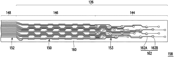
a conductive line extending along the dielectric layer, the conductive line having a first meandering portion and a straight portion, the first meandering portion disposed in the first edge region, the straight portion extending above the encapsulant, the first meandering portion connecting the straight portion to the first conductive via.
|