| CPC H01L 21/8221 (2013.01) [H01L 21/0217 (2013.01); H01L 21/02178 (2013.01); H01L 21/2252 (2013.01); H01L 21/26533 (2013.01); H01L 21/6835 (2013.01); H01L 21/762 (2013.01); H01L 21/823431 (2013.01); H01L 21/823437 (2013.01); H01L 21/823481 (2013.01); H01L 27/0886 (2013.01); H01L 29/167 (2013.01); H01L 29/401 (2013.01); H01L 29/66545 (2013.01); H01L 2221/6835 (2013.01)] | 20 Claims |
|
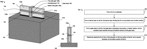
1. A method comprising:
forming a fin on a substrate;
forming a dielectric layer comprising a fixed charge along a central region of the fin, the dielectric layer dividing the fin into a first section above the dielectric layer and a second section below the dielectric layer;
selectively doping the first section of the fin to form one or more first transistors on the first section of the fin; and
selectively doping the second section of the fin to form one or more second transistors on the second section of the fin.
|