| CPC H01L 21/76831 (2013.01) [H01L 21/76832 (2013.01); H01L 21/76879 (2013.01); H01L 23/53238 (2013.01)] | 20 Claims |
|
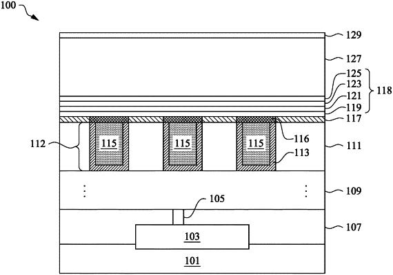
1. A method of forming a semiconductor device, the method comprising:
forming a first conductive feature in a first dielectric layer disposed over a substrate;
forming a metal cap layer over an upper surface of the first conductive feature distal from the substrate;
selectively forming a dielectric cap layer over an upper surface of the first dielectric layer and laterally adjacent to the metal cap layer, wherein the metal cap layer is exposed by the dielectric cap layer; and
forming an etch stop layer stack over the metal cap layer and the dielectric cap layer, wherein the etch stop layer stack comprises a plurality of etch stop layers.
|