| CPC H01L 21/76251 (2013.01) [H01L 21/0245 (2013.01); H01L 21/02488 (2013.01); H01L 21/02658 (2013.01); H01L 21/324 (2013.01); H01L 27/1203 (2013.01)] | 11 Claims |
|
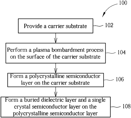
1. A method of fabricating a semiconductor substrate, comprising:
providing a carrier substrate including a surface;
performing a plasma treatment on the surface of the carrier substrate;
forming a polycrystalline semiconductor layer on the surface of the carrier substrate;
performing a rapid thermal treatment on the polycrystalline semiconductor layer;
forming a buried dielectric layer on the polycrystalline semiconductor layer; and
forming a single crystalline semiconductor layer on the buried dielectric layer,
wherein the polycrystalline semiconductor layer comprises an upper region adjacent to the buried dielectric layer and a lower region away from the buried dielectric layer, and when the rapid thermal treatment is performed on the polycrystalline semiconductor layer, an increase in resistivity of the upper region is greater than an increase in resistivity of the lower region.
|