| CPC H01L 21/561 (2013.01) [H01L 21/568 (2013.01); H01L 23/552 (2013.01)] | 7 Claims |
|
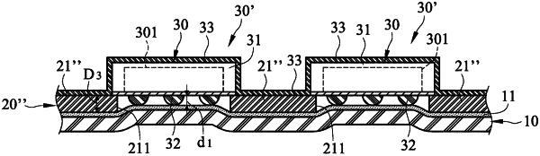
1. A semiconductor packaging structure with a back-deposited shielding layer comprising:
a substrate having an adhesive layer;
a grid adhered to the adhesive layer of the substrate and having multiple frames;
multiple semiconductor devices, and each semiconductor device corresponding to one of the frames and having
a body having a first surface, a second surface, a third surface, a fourth surface, a fifth surface and a sixth surface, wherein
the first surface faces the adhesive layer of the substrate and is distant from the adhesive layer at a first distance;
a thickness of each frame of the grid is larger than the first distance;
a second distance is disposed between a periphery of the first surface and the corresponding frame; and
the second distance is smaller than the first distance; and
multiple solder balls disposed on the first surface, aligning with an opening of the corresponding frame and adhered to a portion of the adhesive layer in the opening; and
a metal layer forming on the grid and the second to sixth surfaces of the bodies of the semiconductor devices.
|