| CPC H01L 21/2022 (2013.01) [H01L 21/02002 (2013.01); H01L 21/0243 (2013.01); H01L 21/0245 (2013.01); H01L 21/0262 (2013.01); H01L 21/02381 (2013.01); H01L 21/02502 (2013.01); H01L 21/02516 (2013.01); H01L 21/02532 (2013.01); H01L 21/02579 (2013.01); H01L 21/02636 (2013.01); H01L 21/02639 (2013.01); H01L 29/045 (2013.01); H01L 29/0847 (2013.01); H01L 29/165 (2013.01); H01L 29/66287 (2013.01); H01L 29/66628 (2013.01); H01L 29/66636 (2013.01); H01L 29/7848 (2013.01); H01L 21/30608 (2013.01)] | 20 Claims |
|
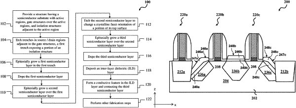
1. A device comprising:
a first gate structure disposed over a substrate;
an isolation structure at least partially embedded in the substrate;
a first source/drain feature associated with the first gate structure, the first source/drain feature including:
a first semiconductor layer disposed on the substrate;
a second semiconductor layer disposed on the first semiconductor layer and interfacing with the isolation structure; and
a third semiconductor layer disposed on the second semiconductor layer and interfacing with the isolation structure; and
an inter-layer dielectric (ILD) layer disposed over the isolation structure and the first gate structure, wherein the ILD layer interfaces with a sidewall of the isolation structure.
|