| CPC H01L 21/02129 (2013.01) [H01L 21/0217 (2013.01); H01L 21/02274 (2013.01); H01L 21/76802 (2013.01); H01L 21/76877 (2013.01); H01L 29/401 (2013.01); H01L 29/42368 (2013.01)] | 18 Claims |
|
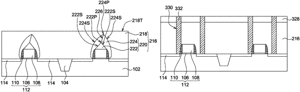
1. A method for forming a semiconductor structure, comprising:
forming a gate by a method comprising:
forming a gate dielectric layer on a substrate;
forming a gate electrode on the gate dielectric layer;
forming a nitride spacer on a sidewall of the gate electrode; and
forming a phosphorus containing dielectric layer on the gate, wherein the phosphorus containing dielectric layer has a varied phosphorus dopant density distribution profile, the phosphorus containing dielectric layer comprises:
a first phosphorus dopant density region on the gate and having a top point; and
a second phosphorus dopant density region on the first phosphorus dopant density region and having another top point, wherein a straight line defined between the top point of the first phosphorus dopant density region and the another top point of the second phosphorus dopant density region is deviated from a vertical direction.
|