| CPC H01L 21/02016 (2013.01) [H01L 21/02019 (2013.01)] | 17 Claims |
|
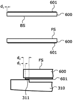
1. A method of treating a semiconductor wafer comprising monocrystalline silicon, having two sides and an edge, comprising:
disposing the semiconductor wafer on a susceptor in a coating apparatus and then processing the semiconductor wafer in said coating apparatus by passing an etching gas comprising hydrogen chloride or a mixture of hydrogen chloride and hydrogen into the coating apparatus in an etching step during said processing, and coating only one side of the two sides of the semiconductor wafer with a protective layer, either before said processing of a first side of the semiconductor wafer which has been subjected to a polishing operation by chemical mechanical polishing or before processing a second side of the semiconductor wafer opposite the first side.
|