| CPC H01J 37/32477 (2013.01) [C23C 16/06 (2013.01); C23C 16/4404 (2013.01); C23C 16/45536 (2013.01); C23C 16/45544 (2013.01); C23C 16/45565 (2013.01); H01J 37/32467 (2013.01); H01L 21/28556 (2013.01); H01L 21/67017 (2013.01); H01J 2237/3321 (2013.01)] | 17 Claims |
|
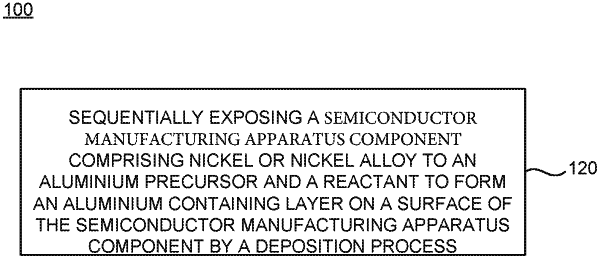
1. A method of depositing a coating on a semiconductor manufacturing apparatus component using an atomic layer deposition process, comprising:
1) in a deposition reactor, contacting a semiconductor manufacturing apparatus component comprising nickel or nickel alloy with an aluminum precursor; followed by
2) contacting the semiconductor manufacturing apparatus component comprising nickel or nickel alloy with a reactant; followed by
3) purging the deposition reactor; followed by
repeating 1, 2, and 3 to form an aluminum containing layer on a surface of the semiconductor manufacturing apparatus component comprising nickel or nickel alloy; and
annealing the aluminum containing layer at a temperature of up to 1000 degrees Celsius in a nitrogen atmosphere.
|