US 11,658,003 B2
Method for producing phosphor panel, phosphor panel, image intensifier and scanning-type electronic microscope
Yasumasa Hamana, Hamamatsu (JP); Hiroyuki Watanabe, Hamamatsu (JP); Kenshi Shimano, Hamamatsu (JP); and Hiroji Nishizawa, Hamamatsu (JP)
Assigned to HAMAMATSU PHOTONICS K.K., Hamamatsu (JP)
Appl. No. 17/430,019
Filed by HAMAMATSU PHOTONICS K.K., Hamamatsu (JP)
PCT Filed Nov. 22, 2019, PCT No. PCT/JP2019/045826
§ 371(c)(1), (2) Date Aug. 11, 2021,
PCT Pub. No. WO2020/170532, PCT Pub. Date Aug. 27, 2020.
Claims priority of application No. JP2019-028122 (JP), filed on Feb. 20, 2019.
Prior Publication US 2022/0148848 A1, May 12, 2022
Int. Cl. H01J 37/22 (2006.01); H01J 9/22 (2006.01)
CPC H01J 37/224 (2013.01) [H01J 9/22 (2013.01)] 13 Claims
OG exemplary drawing
 
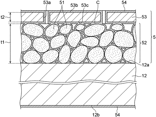
1. A method of manufacturing a phosphor panel, comprising:
forming a phosphor layer having a plurality of phosphor particles on a light transmissive substrate;
forming an organic film on the phosphor layer;
forming a metal reflection film on the organic film;
removing the organic film by firing;
forming an oxide film integrally covering a surface of the metal reflection film and surfaces of the phosphor particles by atomic layer deposition.