| CPC H01F 27/24 (2013.01) [H01F 27/292 (2013.01); H01F 41/0233 (2013.01); H01L 23/495 (2013.01); H01L 24/48 (2013.01); H01L 24/73 (2013.01); H01L 25/16 (2013.01); H01L 2224/48463 (2013.01); H01L 2924/30107 (2013.01)] | 7 Claims |
|
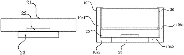
1. A switching power supply module, comprising a power inductor and a switching power supply chip, wherein the power inductor comprises a magnetic core and L-shaped metal end electrodes welded at two ends of the magnetic core, and the switching power supply chip comprises a packaging body, a bare chip in the packaging body, and a bottom bonding pad of the bare chip;
the L-shaped metal end electrode comprises a first electrode part and a second electrode part which are perpendicular to each other, the first electrode part is welded to the magnetic core and at a right angle to the magnetic core, and the second electrode part extends in parallel from the first electrode part to the middle of the magnetic core; and
the bare chip and the packaging body thereof are together embedded between the first electrode part, the second electrode part and the magnetic core; meanwhile, the bottom bonding pad abuts between two second electrode parts and is insulated from the second electrode part, and the weld face of the bottom bonding pad is flush with the weld face of the second electrode part;
wherein the packaging body of the bare chip is a resin packaging body, and the outline of the outer shape of the packaging body is matched with a gap formed between the L-shaped metal end electrode and the magnetic core.
|