| CPC G11C 14/0081 (2013.01) [G11C 11/161 (2013.01); G11C 11/1659 (2013.01); G11C 11/1675 (2013.01); G11C 11/419 (2013.01)] | 20 Claims |
|
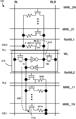
1. An integrated circuit comprising:
a first static random access memory (SRAM) having a first port and a second port;
a first set of magnetic tunnel junction (MTJ) cells, each of the first set of MTJ cells and a corresponding one of a first set of pass transistors coupled to each other in series between a first select line and the second port of the first SRAM, wherein the first set of MTJ cells includes a first reference MTJ cell having two electrodes coupled to the first select line and a first reference line, respectively;
a second set of MTJ cells, each of the second set of MTJ cells and a corresponding one of a second set of pass transistors coupled to each other in series between a second select line and the first port of the first SRAM, wherein the second set of MTJ cells includes a second reference MTJ cell having two electrodes coupled to the second select line and a second reference line, respectively;
wherein the first set of MTJ cells each store a first bit independent of a second bit that the second set of MTJ cells each store.
|