| CPC G09G 3/3225 (2013.01) [G09G 2300/0413 (2013.01); G09G 2300/0426 (2013.01); G09G 2300/0819 (2013.01); G09G 2300/0842 (2013.01); G09G 2300/0861 (2013.01); G09G 2320/0233 (2013.01); G09G 2330/04 (2013.01)] | 18 Claims |
|
1. A display panel, comprising:
a display region; and
a non-display region surrounding the display region,
wherein the display region comprises:
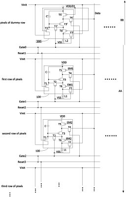
a plurality of sub-pixels disposed in an array, each sub-pixel comprises a pixel circuit and a light emitting device, and the pixel circuit is used to drive the light emitting device to emit light; the pixel circuit comprises a drive transistor, an anode reset transistor, and a reset transistor, a first terminal of the anode reset transistor is electrically connected with an initialization signal line, a second terminal of the anode reset transistor is electrically connected with an anode of the light emitting device, and a cathode of the light emitting device is electrically connected with a first power terminal; a first terminal of the reset transistor is electrically connected with a gate of the drive transistor, and a second terminal of the reset transistor is electrically connected with the initialization signal line;
a control terminal of the anode reset transistor in one sub-pixel in one column of the sub-pixels is electrically connected with a control terminal of the reset transistor in another sub-pixel in the one column of the sub-pixels, wherein the one sub-pixel and the another sub-pixel are in adjacent rows of the sub-pixels;
the non-display region comprises:
a row of dummy sub-pixels, the dummy sub-pixels correspond to columns of the sub-pixels in one to one correspondence, each dummy sub-pixel comprises a dummy pixel circuit and a dummy light emitting device, and the dummy light emitting device does not emit light; the dummy pixel circuit comprises a dummy anode reset transistor, a first terminal of the dummy anode reset transistor is electrically connected with the initialization signal line, a second terminal of the dummy anode reset transistor is electrically connected with an anode of the dummy light emitting device, and a cathode of the dummy light emitting device is electrically connected with the first power terminal; and
a control terminal of the dummy anode reset transistor is correspondingly electrically connected with the control terminal of the reset transistor in a respective one sub-pixel in a first row of the sub-pixels.
|