| CPC G09G 3/2092 (2013.01) [G09G 3/3266 (2013.01); G09G 2310/0286 (2013.01); G09G 2310/08 (2013.01); G09G 2330/04 (2013.01); G11C 19/28 (2013.01)] | 21 Claims |
|
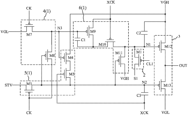
1. A drive circuit, comprising:
a control module electrically connected to a start signal line, a first clock signal line, a second clock signal line, a first potential signal line, a second potential signal line, a first node, and a second node, wherein the drive circuit has a first state and a display state, wherein the first state is prior to the display state, and the control module is configured to transmit a voltage signal to the first node and the second node in response to a first clock signal and a second clock signal;
an output module electrically connected to the first potential signal line, the second potential signal line, an output wire, the first node, and the second node, wherein the output module is configured to transmit a voltage signal to the output wire in response to a control signal of the first node and a control signal of the second node; and
a protect module, wherein in the first state, the protect module is configured to transmit an effective voltage signal to the first node in response to a control signal in such a manner that the output module transmits an ineffective voltage signal to the output wire,
wherein the control module comprises:
a third control unit electrically connected to the second clock signal line, the first node, the second node, and a third node, and configured to transmit a voltage signal to the first node in response to a voltage signal of the third node, the second clock signal, and the voltage signal of the second node; and
wherein the third control unit comprises:
a ninth transistor comprising a control electrode electrically connected to the third node, a first electrode electrically connected to the second clock signal line, and a second electrode;
a tenth transistor comprising a control electrode electrically connected to the second clock signal line, a first electrode electrically connected to the second electrode of the ninth transistor, and a second electrode electrically connected to the first node;
an eleventh transistor comprising a control electrode electrically connected to the second node, a first electrode electrically connected to the second potential signal line, and a second electrode electrically connected to the first node; and
a first capacitor comprising a first plate electrically connected to the third node, and a second plate electrically connected to the second electrode of the ninth transistor.
|