| CPC G09G 3/2074 (2013.01) [G09G 2310/0272 (2013.01); G09G 2310/0286 (2013.01); G09G 2330/028 (2013.01)] | 20 Claims |
|
1. A display substrate, comprising:
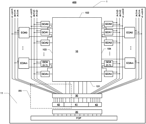
a base substrate comprising an active area and a peripheral area surrounding the active area;
a plurality of sub-pixels located in the active area;
a plurality of data lines located in the active area and extending in a first direction, wherein the plurality of data lines are electrically coupled to the plurality of sub-pixels;
a plurality of gate lines located in the active area and extending in a second direction, wherein the first direction intersects the second direction, and the plurality of gate lines are electrically coupled to the plurality of sub-pixels;
a gate driving circuit located in the peripheral area, and electrically coupled to the plurality of gate lines;
a first start-up voltage signal line, a first clock signal line, and a second clock signal line electrically coupled to the gate driving circuit;
a plurality of first pins located in the peripheral area;
a plurality of second pins located in the peripheral area and between the active area and the plurality of first pins;
a plurality of first array test pins located between the plurality of first pins and the plurality of second pins, wherein the plurality of first array test pins are electrically coupled respectively to a plurality of array test signal lines, and the plurality of array test signal lines comprise at least one of the first start-up voltage signal line, the first clock signal line, or the second clock signal line; and
a plurality of second array test pins located between the plurality of first pins and the plurality of second pins and arranged in a direction along a boundary of the active area, wherein the plurality of first array test pins are located on at least one side of the plurality of second array test pins in the direction along the boundary of the active area, the plurality of second array test pins are electrically coupled to the plurality of data lines, and the plurality of the second array test pins are configured to receive array test data signals from the plurality of sub-pixels through the plurality of data lines.
|