| CPC G09G 3/006 (2013.01) [G09G 3/3258 (2013.01); G09G 3/3275 (2013.01); G09G 2320/04 (2013.01); G09G 2330/12 (2013.01)] | 20 Claims |

|
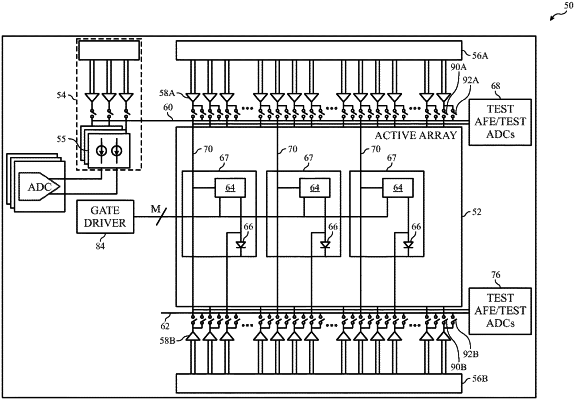
1. An electronic display comprising:
an active array comprising a pixel circuit;
a source driver configured to be coupled to and provide a voltage to the pixel circuit; and
a comparator coupled to the pixel circuit and configured to receive a reference voltage and the voltage from the pixel circuit, wherein the reference voltage comprises a threshold voltage for the pixel circuit, and wherein the comparator is configured to identify a defective source driver.
|
|
8. An electronic display comprising:
an active array comprising a pixel circuit coupled to a light-emitting diode (LED);
a data line coupled to the pixel circuit;
a test bus configured to be coupled to an anode of the LED and configured to receive a voltage at a cathode of the LED as input voltage; and
test circuitry coupled to the test bus and configured to determine that the LED is defective based on a comparison of a voltage at the anode and the voltage at the cathode.
|
|
15. An electronic display comprising:
an active array comprising a plurality of pixel circuitries arranged in rows, each row coupled to a data line;
a plurality of gate drivers;
a first plurality of switches configured to couple the plurality of gate drivers to respective data lines;
a second plurality of switches configured to couple data lines of adjacent gate drivers;
a third plurality of switches opposite the second plurality of switches and configured to couple data lines of adjacent gate drivers; and
test circuitry configured to identify a defective gate driver, a defective pixel circuitry, or a defective data line, or any combination thereof.
|