| CPC G06F 13/4286 (2013.01) [G06F 5/065 (2013.01); H04L 69/14 (2013.01); H04L 49/25 (2013.01)] | 20 Claims |
|
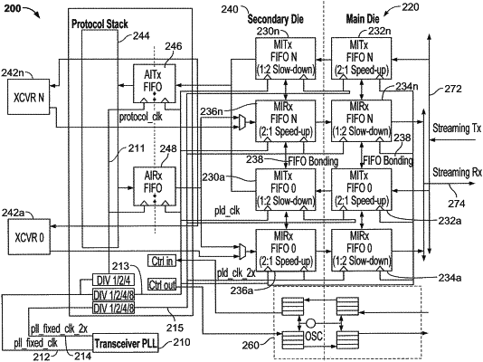
1. A multi-die electronic device comprising:
a communication bus comprising a plurality of channels and a clock signal line;
an input/output (IO) die comprising:
a first bus interface coupled to the communication bus, wherein the first bus interface is configurable to transmit source synchronous data comprising a plurality of data signals over a first plurality of unidirectional channels of the plurality of channels;
a second bus interface to couple the IO die to a memory; and
an on-die interconnect to couple the first bus interface to the second bus interface; and
an integrated circuit die comprising a third bus interface to couple the integrated circuit die to the first bus interface over the communication bus and receive the plurality of data signals via the first plurality of unidirectional channels, wherein the third bus interface comprises circuitry to synchronize the plurality of data signals of the source synchronous data by latching the received source synchronous data using a clock signal transmitted from the first bus interface over the clock signal line;
wherein a clock frequency associated with the second bus interface and a clock frequency associated with the on-die interconnect are separately settable; and
wherein, in a first configuration, the clock frequency associated with the second bus interface is different from the clock frequency associated with the on-die interconnect, and in a second configuration, the clock frequency associated with the on-die interconnect and the clock frequency associated with the second bus interface are the same.
|