| CPC G06F 13/1615 (2013.01) [G06F 13/1689 (2013.01)] | 20 Claims |
|
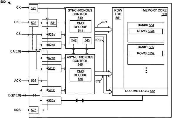
1. A memory controller, comprising:
a first timing signal interface to transmit a first timing signal to a memory device having a memory core that determines a synchronous sampling of signals by the memory device at a first set of links;
a second timing signal interface to transmit a second timing signal that determines a synchronous sampling of signals by the memory device at a second set of links; and,
mode control circuitry to operate the memory device in a first mode where the memory device accesses the memory core in response to at least first command, first control, and first address information received via a first synchronous sampling of signals at the first set of links using the first timing signal, the mode control circuitry to also operate the memory device in a second mode where the memory device accesses the memory core in response to second command, second control, and second address information received via a first asynchronous sampling of signals at the first set of links and the first asynchronous sampling of signals at the second set of links using a third timing signal transmitted via a third timing signal interface.
|