| CPC G06F 3/0421 (2013.01) [G06F 3/04166 (2019.05); G09G 3/3266 (2013.01); G09G 3/3275 (2013.01); G09G 3/3677 (2013.01); G09G 3/3688 (2013.01); G09G 2354/00 (2013.01)] | 19 Claims |
|
1. An array substrate, comprising a thin film transistor (TFT) backplane, wherein the TFT backplane comprises:
a substrate; and
a light sensitive touch control sub-circuit and a light emitting driving control sub-circuit of a pixel circuit arranged on the substrate; and
a light emitting device of the pixel circuit on the substrate in a light outgoing direction of the array substrate, wherein the light emitting device is a top emission light emitting device,
wherein the light sensitive touch control sub-circuit comprises a light sensitive transistor,
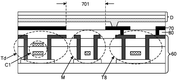
the array substrate further comprises a light shading layer between the substrate and the light emitting device in a sub-pixel area where the pixel circuit is arranged,
the light shading layer comprises a hollowed-out area exposing the light sensitive transistor,
a planarization layer is between the light shading layer and the substrate, and
an orthographic projection of the light sensitive transistor on the substrate overlaps with an orthographic projection of the planarization layer on the substrate,
the TFT backplane further comprises a driving sub-circuit included in the light emitting driving control sub-circuit, the driving sub-circuit comprises a driving transistor and a first capacitor,
wherein an active layer of the driving transistor and an active layer of the light sensitive transistor are located on a same layer, and are both directly disposed on the substrate, and
the driving transistor and the first capacitor are located between the substrate and the light shading layer, orthographic projections of the first capacitor and the driving transistor on the substrate are within an orthographic projection of the light shading layer on the substrate.
|