| CPC G06F 3/0412 (2013.01) [G06F 3/044 (2013.01); G06F 3/0443 (2019.05); G06F 3/0446 (2019.05); G06F 3/04164 (2019.05); G09G 3/3225 (2013.01); H01L 27/323 (2013.01); H01L 27/3246 (2013.01); H01L 27/3276 (2013.01); H01L 51/5246 (2013.01); H01L 51/5253 (2013.01); H01L 51/5256 (2013.01); H01L 51/56 (2013.01); G06F 2203/04102 (2013.01); G06F 2203/04103 (2013.01); G06F 2203/04111 (2013.01); G09G 3/20 (2013.01); G09G 2310/0264 (2013.01); H01L 27/3206 (2013.01)] | 14 Claims |
|
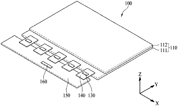
1. A display device comprising:
a first substrate including a display area on which pixels are arranged and a non-display area including a pad area and a bending area disposed between the pad area and the display area;
a dam disposed between the bending area and the display area;
a pad electrode disposed at the pad area;
an encapsulation film including a first inorganic film, a second inorganic film on the first inorganic film, and an organic film between the first inorganic film and the second inorganic film, and the organic film of the encapsulation film covers the display area;
an organic pattern disposed between the dam and the pad electrode;
a touch sensing layer disposed on the second inorganic film;
a touch line being electrically connected with the touch sensing layer; and
a connection line being electrically connected to the pad electrode and the touch line, and including first, second and third connection lines,
wherein the second connection line is electrically connected with one side of the first connection line, and the third connection line is disposed on the same layer as the second connection line, spaced apart from the second connection line and electrically connected with the other side of the first connection line, and
wherein the organic pattern is disposed on an upper portion of the third connection line.
|