| CPC G02F 1/136209 (2013.01) [G02F 1/1368 (2013.01); G02F 1/136286 (2013.01)] | 11 Claims |
|
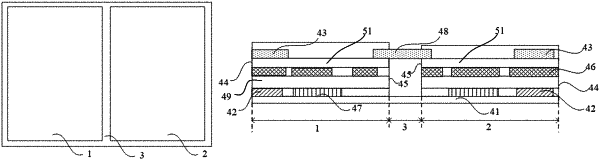
1. A display panel, comprising a first display sub-panel, a second display sub-panel spliced with the first display sub-panel and a light-shielding layer, wherein a gap region exists between the first display sub-panel and the second display sub-panel, the light-shielding layer is at least located in the gap region,
the first display sub-panel and the second display sub-panel each comprise a plurality of pixel units arranged in an array, and each pixel unit at least comprises:
a substrate;
a data line located on the substrate;
a black matrix located on a side of the data line away from the substrate, wherein an orthographic projection of the data line on the substrate falls within an orthographic projection of the black matrix on the substrate, in at least one of the first display sub-panel and the second display sub-panel, the black matrix of the pixel unit closest to the gap region and the light-shielding layer are arranged with an interval therebetween, and the black matrix is located on a side away from the gap region in the pixel unit,
wherein the light-shielding layer extends from the gap region into the first display sub-panel and the second display sub-panel, respectively;
each of the pixel units further comprises a common electrode located on a side of the data line away from the substrate, wherein in each of the first display sub-panel and the second display sub-panel, an orthogonal projection of the common electrode of the pixel unit closest to the gap region on the substrate overlaps an orthogonal projection of the light-shielding layer on the substrate.
|