| CPC G01N 21/66 (2013.01) [G01N 21/8806 (2013.01); G01N 2201/062 (2013.01)] | 24 Claims |
|
1. An inspection method for inspecting light-emitting diodes, comprising
providing a light-emitting diode wafer comprising a plurality of light-emitting diodes, wherein the light-emitting diode wafer comprises a plurality of scan regions, each of the scan regions has a plurality of first light-emitting diodes of the plurality of light-emitting diodes, the scan regions comprise m scan regions, the m scan regions comprise a 1st scan region to a mth scan region, and m is a positive integer greater than or equal to 2;
scanning the 1st scan region to the mth scan region of the light-emitting diode wafer to respectively obtain 1st relative height information to mth relative height information corresponding to the 1st scan region to the mth scan region;
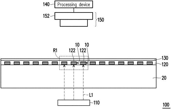
the light-emitting diode wafer comprising a plurality of to-be-inspected regions, each of the to-be-inspected regions comprising a plurality of second light-emitting diodes of the plurality of light-emitting diodes, measuring a 1st real-time distance between a photoelectric sensing structure of a sensing probe and one of the to-be-inspected regions of the light-emitting diode wafer and adjusting a distance between the photoelectric sensing structure of the sensing probe and the to-be-inspected region of the light-emitting diode wafer to a target distance according to the 1st real-time distance;
allowing an illumination beam to simultaneously irradiate the plurality of second light-emitting diodes of the to-be-inspected region to generate a first charge distribution, a first electric field distribution, or a first voltage distribution on the plurality of second light-emitting diodes of the to-be-inspected region due to a photovoltaic effect caused by the illumination beam;
using the sensing probe to measure the first charge distribution, the first electric field distribution, or the first voltage distribution on the plurality of second light-emitting diodes of the to-be-inspected region to determine a plurality of first electro-optical characteristics of the plurality of second light-emitting diodes of the to-be-inspected region when the target distance between the photoelectric sensing structure of the sensing probe and the to-be-inspected region of the light-emitting diode wafer is kept;
adjusting a distance between the photoelectric sensing structure of the sensing probe and a next to-be-inspected region of the light-emitting diode wafer to the target distance according to at least two of the 1st relative height information to the mth relative height information;
allowing the illumination beam to simultaneously irradiate the plurality of second light-emitting diodes of the next to-be-inspected region to generate a second charge distribution, a second electric field distribution, or a second voltage distribution on the plurality of second light-emitting diodes of the next to-be-inspected region due to the photovoltaic effect caused by the illumination beam; and
using the sensing probe to measure the second charge distribution, the second electric field distribution, or the second voltage distribution on the plurality of second light-emitting diodes of the next to-be-inspected region to determine a plurality of second electro-optical characteristics of the plurality of second light-emitting diodes of the next to-be-inspected region when the target distance between the photoelectric sensing structure of the sensing probe and the next to-be-inspected region of the light-emitting diode wafer is kept.
|