| CPC B81B 3/0005 (2013.01) [B81C 1/00968 (2013.01); B81C 2201/112 (2013.01); B81C 2201/115 (2013.01)] | 20 Claims |
|
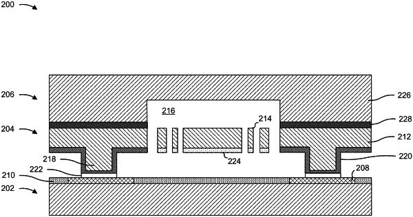
8. A micro-electromechanical-system (MEMS) device, comprising:
a capping wafer;
a circuitry wafer comprising a metal bonding pad;
a device wafer, between the capping wafer and the circuitry wafer, comprising:
a support structure, and
a germanium bonding pad between the metal bonding pad and the support structure;
one or more moveable MEMS structures in a cavity formed by the capping wafer, the circuitry wafer, and the device wafer;
a first polysilicon layer on a bottom surface of the one or more moveable MEMS structures; and
a second polysilicon layer between the support structure and the germanium bonding pad,
wherein a surface roughness of the first polysilicon layer is different from a surface roughness of the second polysilicon layer.
|