| CPC H10N 70/8265 (2023.02) [H10B 63/84 (2023.02); H10N 70/023 (2023.02); H10N 70/026 (2023.02); H10N 70/063 (2023.02); H10N 70/231 (2023.02); H10N 70/841 (2023.02); H10N 70/861 (2023.02); H10N 70/882 (2023.02)] | 6 Claims |
|
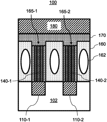
1. A semiconductor device comprising:
a substrate;
at least one lower electrode disposed within the substrate;
a pillar disposed on the lower electrode, the pillar including a PCM layer and sidewall liners;
dielectric layer portions disposed on the substrate adjacent to the sidewall liners, each of the dielectric layer portions including an air gap to reduce thermal cross-talk between adjacent bits, wherein an upper surface of the pillar that is opposite a side of the pillar that is closest to the substrate is vertically offset from the upper surface of the dielectric layer portions;
a selector layer directly disposed on the pillar and the dielectric layer portions, the selector layer having a stepped interface that is conformal with the vertically offset upper surface of the pillars and the uppers surface of the dielectric layer portions; and
an upper electrode disposed on the selector layer.
|