US 11,968,910 B2
Semiconductor device and method for fabricating the same
Hung-Chan Lin, Tainan (TW); Yu-Ping Wang, Hsinchu (TW); and Chien-Ting Lin, Tainan (TW)
Assigned to UNITED MICROELECTRONICS CORP., Hsin-Chu (TW)
Filed by UNITED MICROELECTRONICS CORP., Hsin-Chu (TW)
Filed on Oct. 14, 2021, as Appl. No. 17/500,971.
Claims priority of application No. 202111067661.2 (CN), filed on Sep. 13, 2021.
Prior Publication US 2023/0084241 A1, Mar. 16, 2023
Int. Cl. H10N 52/01 (2023.01); H10B 61/00 (2023.01); H10N 52/00 (2023.01); H10N 52/80 (2023.01)
CPC H10N 52/01 (2023.02) [H10B 61/00 (2023.02); H10N 52/00 (2023.02); H10N 52/80 (2023.02)] 15 Claims
OG exemplary drawing
 
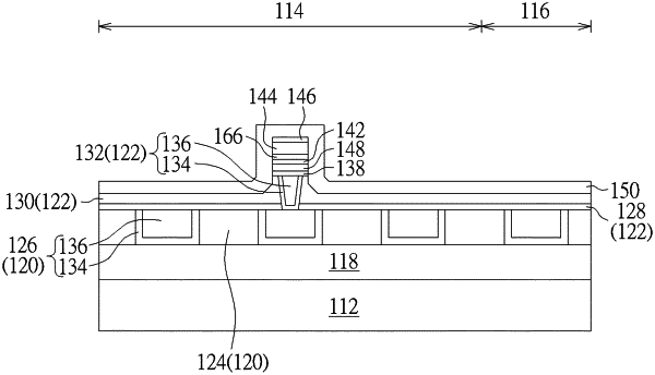
1. A method for fabricating a semiconductor device, comprising:
forming a magnetic tunneling junction (MTJ) stack on a substrate;
forming a top electrode on the MTJ stack;
forming an etch stop layer on the top electrode;
forming a first spin orbit torque (SOT) layer on the etch stop layer; and
patterning the first SOT layer, the etch stop layer, and the MTJ stack to form a MTJ.