| CPC H10N 50/80 (2023.02) [G11C 11/161 (2013.01); H10B 61/20 (2023.02); H10N 50/01 (2023.02); G11C 11/1655 (2013.01); G11C 11/1657 (2013.01); H10N 50/85 (2023.02)] | 20 Claims |

|
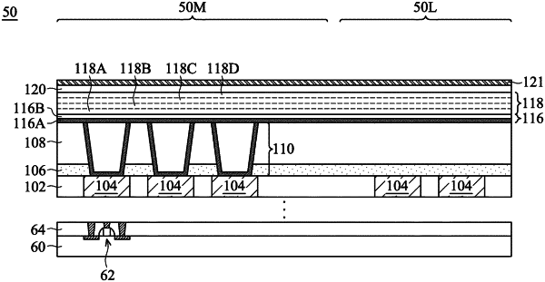
1. A device comprising:
a first inter-metal dielectric over a semiconductor substrate, the semiconductor substrate comprising active devices;
a first conductive feature extending through the first inter-metal dielectric, the first conductive feature electrically connected to the active devices;
a first bottom electrode over the first conductive feature;
a first magnetic tunnel junction stack over the first bottom electrode;
a first top electrode comprising:
a first conductive layer over the first magnetic tunnel junction stack;
a dielectric layer over the first conductive layer; and
a second conductive layer over the dielectric layer;
a second inter-metal dielectric over the first top electrode; and
a second conductive feature extending through the second inter-metal dielectric, the second conductive feature contacting the first top electrode.
|