| CPC H10K 85/633 (2023.02) [H10K 85/324 (2023.02); H10K 85/342 (2023.02); H10K 85/346 (2023.02); H10K 85/348 (2023.02); H10K 85/622 (2023.02); H10K 85/623 (2023.02); H10K 85/653 (2023.02); H10K 85/654 (2023.02); H10K 85/656 (2023.02); H10K 85/6572 (2023.02); H10K 85/6574 (2023.02); H10K 85/6576 (2023.02); H10K 50/11 (2023.02); H10K 50/15 (2023.02); H10K 50/16 (2023.02); H10K 50/171 (2023.02); H10K 2101/40 (2023.02)] | 20 Claims |
|
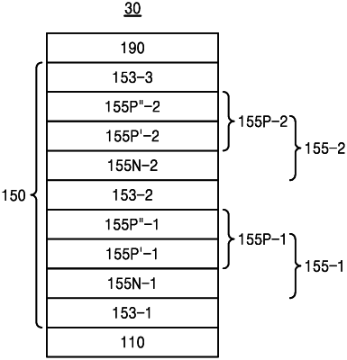
1. An organic light-emitting device comprising:
a first electrode;
a second electrode facing the first electrode;
m light-emitting units stacked between the first electrode and the second electrode and comprising at least one emission layer; and
m−1 charge generating layers, each located between two neighboring light-emitting units of them light-emitting units and comprising an n-type charge generating layer and a p-type charge generation layer,
wherein m is an integer of 2 or more,
at least one of the m−1 p-type charge generation layers comprises a first doping layer and a second doping layer,
the first doping layer comprises a first organic material and a first inorganic material,
the second doping layer comprises a second organic material and a second inorganic material, and
the first inorganic material and the second inorganic material are different from each other.
|