| CPC H10K 59/88 (2023.02) [H01L 23/544 (2013.01); H10K 50/856 (2023.02); H10K 59/131 (2023.02); H10K 59/38 (2023.02); H10K 71/00 (2023.02); H10K 77/10 (2023.02); H01L 2223/54426 (2013.01); H10K 71/851 (2023.02)] | 11 Claims |
|
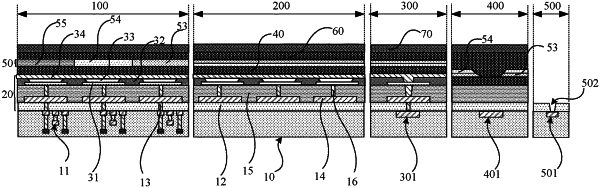
1. A display substrate, comprising: a silicon base substrate and a color film layer disposed on the silicon base substrate, the silicon base substrate containing a plurality of metal traces for connecting a display area and a cathode ring with a bonding area respectively; the color film layer comprising a first align mark, and the first align mark having a hollowed-out structure,
wherein a projection of the first align mark on the silicon base substrate and projections of the metal traces on the silicon base substrate comprise overlapping areas,
wherein the display area comprise a light-emitting structural layer disposed on the silicon base substrate, and the light-emitting structural layer comprises a reflective layer, an anode layer, an organic light-emitting layer and a cathode layer which are sequentially stacked,
wherein a driving circuit layer is disposed in the silicon base substrate in the display area and comprises a first scanning line, a first power line, a data line, a switching transistor and a driving transistor; a control electrode of the switching transistor is connected with the first scanning line, a first electrode of the switching transistor is connected with the data line, a second electrode of the switching transistor is connected with a control electrode of the driving transistor, and a first electrode of the driving transistor is connected with the first power line; the switching transistor is configured to receive a data signal transmitted by the data line under the control of a first scanning signal output by the first scanning line, to make the control electrode of the driving transistor receive the data signals, and the driving transistor is configured to generate a corresponding current at the second electrode under the control of the data signal received by the control electrode thereof, and
wherein the metal traces and the driving circuit layer are disposed on the same layer.
|