| CPC H10K 59/38 (2023.02) [H10K 50/844 (2023.02); H10K 50/865 (2023.02); H10K 59/1213 (2023.02); H10K 59/126 (2023.02); H01L 27/1225 (2013.01); H01L 29/78633 (2013.01); H01L 29/7869 (2013.01)] | 20 Claims |

|
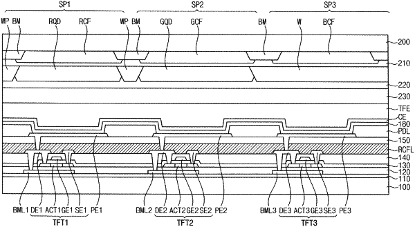
1. A display device comprising:
a base substrate comprising a first sub-pixel area, a second sub-pixel area, and a third sub-pixel area;
first to third thin film transistors on the base substrate and comprising first to third active patterns, respectively;
first to third pixel electrodes electrically connected to the first to third thin film transistors, respectively, and in the first to third sub-pixel areas, respectively;
a blue light emitting layer on the first to third pixel electrodes and configured to emit a blue light;
a first color conversion pattern in the first sub-pixel area on the blue light emitting layer;
a second color conversion pattern in the second sub-pixel area on the blue light emitting layer; and
a red color filter layer between the blue light emitting layer and the first to third active patterns,
wherein, in a plan view, an area, in which the blue light emitting layer overlaps the first to third pixel electrodes, defines a light emitting area, and
wherein the red color filter layer overlaps the defined light emitting area in the plan view.
|