| CPC H10K 59/353 (2023.02) [H10K 50/828 (2023.02); H10K 59/352 (2023.02); H10K 59/60 (2023.02); H10K 2102/102 (2023.02); H10K 2102/103 (2023.02)] | 20 Claims |
|
1. A display substrate comprises:
a first display area comprising a plurality of pixel units, and each of the plurality of pixel units comprising at least three sub-pixel groups emitting light of at least three different colors;
each of the sub-pixel groups comprising at least one sub-pixel, and each sub-pixel comprising a first electrode, a light emitting structure disposed on the first electrode and a second electrode disposed on the light emitting structure; and
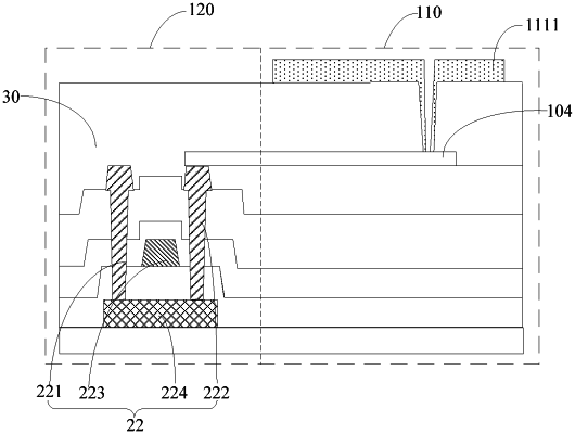
a second display area being adjacent to the first display area, a light transmittance of the second display area being lower than a light transmittance of the first display area; the second display area being provided with a plurality of pixel circuits for driving the sub-pixel groups;
wherein among the sub-pixel groups of each pixel unit in the first display area, at least one first electrode of at least one sub-pixel of at least one sub-pixel group of the pixel unit is electrically connected to at least one corresponding pixel circuit through at least one first connecting portion, and at least one first electrode of at least one sub-pixel of at least one of the other sub-pixel groups of the pixel unit is electrically connected to at least one corresponding pixel circuit through at least one second connecting portion, the at least one first connecting portion and the at least one second connecting portion are disposed in different layers, and the at least one second connecting portion and a plurality of first electrodes of a plurality of sub-pixels of the sub-pixel groups of the pixel unit are disposed in different layers.
|