| CPC H10K 59/353 (2023.02) [G02F 1/136286 (2013.01); H10K 59/131 (2023.02)] | 13 Claims |
|
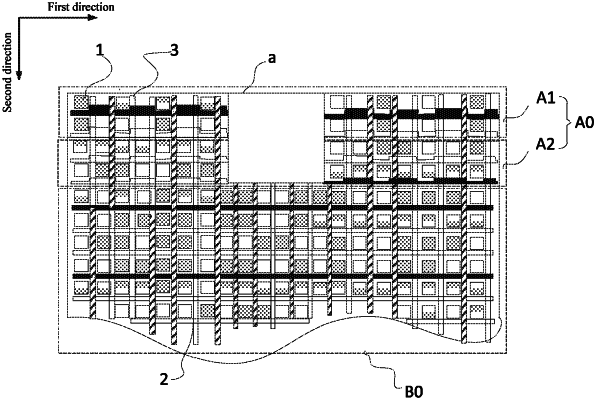
1. A display panel, comprising:
a display region, comprising a first display region and a second display region arranged in a second direction,
wherein the first display region comprises a first sub-display region and a second sub-display region arranged in the second direction, the first sub-display region is located at a side far away from the second display region, and the first sub-display region, the second sub-display region and the second display region each comprise:
a plurality of pixels arranged in an array, wherein a pixel density of the first sub-display region is smaller than a pixel density of the second display region;
a plurality of scanning signal lines, extending in a first direction and arranged in the second direction,
wherein a quantity of pixels electrically connected to each scanning signal line in the first display region is less than a quantity of pixels electrically connected to each scanning signal line in the second display region, and the first direction is intersected with the second direction; and
a plurality of fixed potential signal lines, extending in the second direction and arranged in the first direction,
wherein the scanning signal lines and the fixed potential signal lines are arranged in different layers; in a direction perpendicular to the display panel, a first overlapping region exists between the scanning signal lines and the fixed potential signal lines in the first sub-display region, a second overlapping region exists between the scanning signal lines and the fixed potential signal lines in the second sub-display region, a third overlapping region exists between the scanning signal lines and the fixed potential signal lines in the second display region, and an area of the first overlapping region is at least larger than an area of the third overlapping region;
wherein the pixel density of the first sub-display region is equal to a pixel density of the second sub-display region;
wherein each pixel comprises a light emitting device, and a drive circuit configured to drive the light emitting device; drive circuits of pixels in the first sub-display region are located in the second sub-display region; and the scanning signal lines located in the first sub-display region are electrically connected to corresponding drive circuits located in the second sub-display region.
|