US 11,968,845 B2
Thin film transistor and filter using thin film transistor
Gao-Tian Lu, Beijing (CN); Yang Wei, Beijing (CN); Shou-Shan Fan, Beijing (CN); and Yue-Gang Zhang, Beijing (CN)
Assigned to Tsinghua University, Beijing (CN); and HON HAI PRECISION INDUSTRY CO., LTD., New Taipei (TW)
Filed by Tsinghua University, Beijing (CN); and HON HAI PRECISION INDUSTRY CO., LTD., New Taipei (TW)
Filed on Jan. 17, 2022, as Appl. No. 17/577,131.
Claims priority of application No. 202111026821.9 (CN), filed on Sep. 2, 2021.
Prior Publication US 2023/0060340 A1, Mar. 2, 2023
Int. Cl. H01L 23/00 (2006.01); H03H 11/04 (2006.01); H10K 10/46 (2023.01); H10K 85/20 (2023.01)
CPC H10K 10/474 (2023.02) [H03H 11/04 (2013.01); H10K 10/466 (2023.02); H10K 10/484 (2023.02); H10K 85/221 (2023.02)] 20 Claims
OG exemplary drawing
 
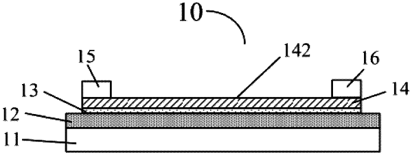
1. A thin film transistor comprising:
a gate electrode;
a carbon nanotube structure;
a gate insulating layer between the gate electrode and the carbon nanotube structure;
a source electrode and a drain electrode electrically insulated from each other and each electrically connected to the carbon nanotube structure; and
an interface charge layer between the carbon nanotube structure and the gate insulating layer, wherein the interface charge layer comprises charges captured by chemical molecular groups or water molecules.