| CPC H10B 61/22 (2023.02) [G11C 11/161 (2013.01); G11C 11/1673 (2013.01); G11C 11/1675 (2013.01); G11C 11/18 (2013.01); H10N 52/00 (2023.02); H10N 52/01 (2023.02); H10N 52/80 (2023.02)] | 20 Claims |
|
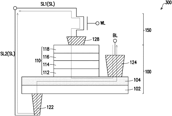
1. A memory device, comprising:
a transistor, disposed on a substrate; and
an interconnect structure, overlying the transistor, wherein the interconnect structure comprises:
a bit line extending along a first direction;
a source line extending along a second direction perpendicular to the first direction; and
a memory cell vertically disposed between the bit line and the source line, wherein the transistor is configured to control a write signal flowing between the bit line and a source of the transistor, and control a read signal flowing between the bit line and a drain of the transistor, wherein the source line is directly under the memory cell, wherein the memory cell comprises:
a selector, electrically coupled to the source of the transistor through the source line;
a magnetic tunnel junction (MTJ) structure, disposed on the selector and electrically coupled to the drain of the transistor; and
a spin orbit torque (SOT) layer, disposed between the selector and the MTJ structure, and electrically coupled to the bit line.
|