| CPC H10B 61/20 (2023.02) [G06F 3/0604 (2013.01); G06F 3/0659 (2013.01); G06F 3/0673 (2013.01); G11C 11/161 (2013.01); G11C 11/1653 (2013.01); G11C 11/1673 (2013.01); G11C 11/1675 (2013.01); H10N 50/01 (2023.02); H10N 50/80 (2023.02)] | 19 Claims |
|
1. A device, comprising:
an integrated circuit chip, the integrated circuit chip including:
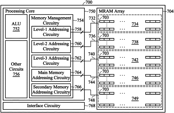
at least one processing core integrated into the chip;
at least one magnetoresistive random access memory (MRAM) circuit integrated into the chip and communicatively coupled to the at least one processing core, the at least one MRAM circuit including a plurality of MRAM cells, wherein the at least one MRAM circuit, in operation, implements,
at least one cache memory via a first region of the plurality of MRAM cells; and
at least one main memory via a second region of the plurality of MRAM cells;
a first addressing circuit positioned in close proximity to the first region of the plurality of MRAM cells and coupled to the first region of the plurality of MRAM cells via a first set of memory control lines, the first addressing circuit corresponding to the first region of the plurality of MRAM cells; and
a second addressing circuit positioned in close proximity to the second region of the plurality of MRAM cells and coupled to the second region of the plurality of MRAM cells via a second set of memory control lines, the second addressing circuit corresponding to the second region of the plurality of MRAM cells, and the second addressing circuit different from the first addressing circuit,
wherein a MRAM cell of the plurality of MRAM cells includes a fixed layer, a free layer and a tunnel barrier layer between the fixed layer and the free layer, the free layer coupled to a first source or drain terminal of a control transistor through a metal layer, the fixed layer coupled to a bit line; and
wherein a second source or drain terminal of the control transistor is coupled to a sense line and a gate of the control transistor is coupled to a write line.
|