| CPC H10B 51/30 (2023.02) [G11C 5/06 (2013.01); H01L 29/516 (2013.01); H01L 29/6684 (2013.01); H01L 29/78391 (2014.09); H01L 29/78618 (2013.01); H10B 51/10 (2023.02)] | 20 Claims |
|
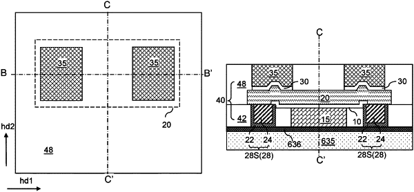
1. A semiconductor structure comprising:
an active layer located over a substrate;
a first gate stack including a stack of a first gate dielectric and a first gate electrode and located on a first surface of the active layer;
a pair of first contact electrodes contacting peripheral portions of the first surface of the active layer and laterally spaced from each other along a first horizontal direction by the first gate electrode;
a second contact electrode contacting a second surface of the active layer that is vertically spaced from the first surface of the active layer; and
a pair of second gate stacks including a respective stack of a second gate dielectric and a second gate electrode and located on a respective peripheral portion of a second surface of the active layer and laterally spaced from each other along the first horizontal direction by the second contact electrode.
|