| CPC H10B 51/20 (2023.02) [H01L 29/0649 (2013.01); H01L 29/78391 (2014.09); H10B 51/10 (2023.02)] | 20 Claims |
|
1. A device comprising:
a semiconductor substrate;
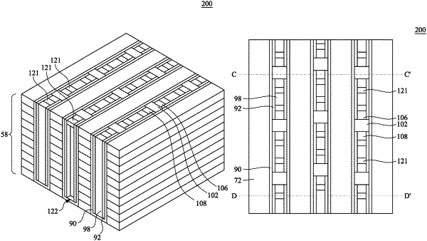
a word line extending over the semiconductor substrate;
a memory film extending along the word line, wherein the memory film contacts the word line;
a channel layer extending along the memory film, wherein the memory film is between the channel layer and the word line;
a plurality of source lines extending along the memory film, wherein the memory film is between the plurality of source lines and the word line;
a plurality of bit lines extending along the memory film, wherein the memory film is between the plurality of bit lines and the word line; and
a plurality of isolation regions, wherein each isolation region of the plurality of isolation regions is between a source line of the plurality of source lines and a bit line of the plurality of the bit lines, wherein each of the isolation regions comprises an air gap and a seal extending over the air gap.
|