| CPC H10B 43/27 (2023.02) [H01L 21/0337 (2013.01); H01L 21/3086 (2013.01); H01L 23/53295 (2013.01); H10B 43/35 (2023.02); H10B 43/40 (2023.02)] | 20 Claims |
|
1. A method for forming a memory device, comprising:
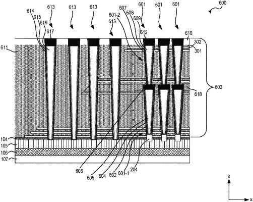
forming a plurality of dielectric stacks stacked on one another over a substrate to create a multiple-stack staircase structure, wherein each one of the plurality of dielectric stacks comprises a plurality of dielectric pairs arranged along a direction perpendicular to a top surface of the substrate;
forming a filling structure over the multiple-stack staircase structure;
forming a semiconductor channel extending through the multiple-stack staircase structure, wherein the semiconductor channel comprises unaligned sidewall surfaces; and
forming a supporting pillar extending through at least one of the multiple-stack staircase structure and the filling structure, wherein the supporting pillar comprises aligned sidewall surfaces.
|