| CPC H10B 41/42 (2023.02) [H01L 21/76229 (2013.01); H01L 29/0649 (2013.01); H01L 29/40114 (2019.08); H01L 29/42368 (2013.01); H01L 29/66545 (2013.01); H01L 29/66825 (2013.01); H01L 29/7883 (2013.01); H10B 41/30 (2023.02); H10B 41/40 (2023.02)] | 20 Claims |
|
1. A method, comprising:
forming an isolation feature in a semiconductor substrate;
depositing a first dielectric layer over and in contact with the semiconductor substrate;
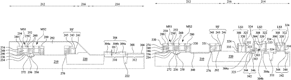
patterning the first dielectric layer to form a first dielectric material over a first portion of the isolation feature and a first portion of the semiconductor substrate at a first side of the isolation feature and a second dielectric material over the first portion of the semiconductor substrate at the first side of the isolation feature and spaced apart from the first dielectric material, recess a second portion of the isolation feature, and expose a second portion of the semiconductor substrate at a second side of the isolation feature, wherein the first and second sides are at opposite sides of the isolation feature, the second portion of the isolation feature is recessed during patterning the first dielectric layer, and the first portion of the isolation feature is between the second portion of the isolation feature and the first portion of the semiconductor substrate;
depositing a second dielectric layer over the semiconductor substrate;
patterning the second dielectric layer, such that the first and second dielectric materials and the patterned second dielectric layer are defined as a concave dielectric layer, and the second portion of the semiconductor substrate and recessed second portion of the isolation feature are exposed from the second dielectric layer;
forming an interfacial layer over the semiconductor substrate;
forming a high-k dielectric layer over the interfacial layer;
depositing a dummy gate layer over the high-k dielectric layer;
patterning the dummy gate layer, the high-k dielectric layer, the interfacial layer, and the concave dielectric layer to form a first gate stack over the first portion of the semiconductor substrate and a second gate stack over the second portion of the semiconductor substrate; and
replacing the patterned dummy gate layer with a conductive layer.
|