| CPC H10B 12/485 (2023.02) [H01L 21/76829 (2013.01); H10B 12/0335 (2023.02); H10B 12/09 (2023.02); H10B 12/315 (2023.02)] | 20 Claims |
|
1. A semiconductor device comprising:
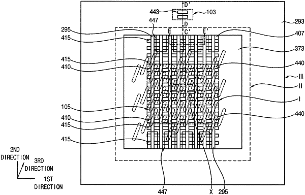
a substrate including a cell region, a peripheral region, and an interface region that is between the cell region and the peripheral region, the cell region including an active pattern, and the interface region including a device isolation pattern and an active pattern;
a gate structure buried in the cell region of the substrate and including a gate mask pattern, the gate mask pattern having a recess;
a first bit line structure including a first portion that is on the cell region of the substrate and a second portion that is on the interface region of the substrate;
a second bit line structure including a third portion that is on the cell region of the substrate and a fourth portion that is on the interface region of the substrate;
a first contact between the first portion of the first bit line structure and the third portion of the second bit line structure;
a first capping pattern between the first portion of the first bit line structure and the third portion of the second bit line structure and adjacent to the first contact;
a second contact between the second portion of the first bit line structure and the fourth portion of the second bit line structure;
a second capping pattern between the second portion of the first bit line structure and the fourth portion of the second bit line structure and adjacent to the second contact; and
a bottom electrode on the first contact,
wherein a bottom surface of the first capping pattern contacts the recess of the gate mask pattern of the gate structure, and
wherein the bottom surface of the first capping pattern is lower than a bottom surface of the second capping pattern.
|