| CPC H10B 12/34 (2023.02) [H10B 12/053 (2023.02); H10B 12/09 (2023.02); H10B 12/315 (2023.02); H10B 12/482 (2023.02); H10B 12/485 (2023.02); H10B 12/50 (2023.02)] | 20 Claims |
|
1. A semiconductor device comprising:
a substrate having a cell region, a peripheral region, and an interface region between the cell region and the peripheral region, the peripheral region including an active pattern, and the interface region including a device isolation layer;
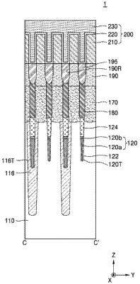
a cell gate structure buried in the substrate of the cell region in a first direction that is parallel to a top surface of the substrate, and extending in the device isolation layer of the interface region of the substrate, the cell gate structure including a gate dielectric layer that is disposed in the substrate, a titanium nitride layer that is disposed on the gate dielectric layer, a doped polysilicon layer that is disposed on the titanium nitride layer, and a cell gate capping layer that is disposed on the doped polysilicon layer;
a bit line structure arranged on the cell region of the substrate in a second direction that is perpendicular to the first direction, and extending on the device isolation layer of the interface region of the substrate, the bit line structure including a bit line pattern, and a bit line capping layer that is disposed on the bit line pattern;
a peripheral gate structure arranged on the peripheral region of the substrate, and including a peripheral gate pattern and a peripheral gate capping layer that is disposed on the peripheral gate pattern;
an insulation layer on the interface region and the peripheral region of the substrate, the insulation layer including a first insulation layer and a second insulation layer that is disposed on the first insulation layer;
a first direct contact on the interface region of the substrate; and
a first wiring on the first direct contact,
wherein the first direct contact is disposed between the bit line structure and the peripheral gate structure, and is disposed in the first insulation layer and the second insulation layer of the insulation layer, and
wherein the first direct contact is in contact with the titanium nitride layer and the doped polysilicon layer of the cell gate structure.
|