| CPC H10B 10/12 (2023.02) [H01L 21/02063 (2013.01); H01L 21/76816 (2013.01); H01L 21/76831 (2013.01); H01L 23/5226 (2013.01); H01L 29/401 (2013.01); H01L 29/41791 (2013.01)] | 20 Claims |
|
1. A method, comprising:
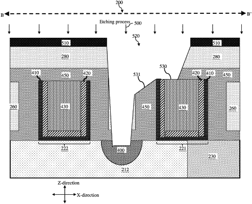
providing a semiconductor device that includes: a fin structure, a source/drain region formed on the fin structure, a gate structure that at least partially wraps around the fin structure, and dielectric materials formed over the source/drain region and over the gate structure;
performing an etching process to the semiconductor device, wherein the etching process forms an opening that extends through the dielectric materials and at least partially exposes both the source/drain region and the gate structure;
forming a polymer layer as a protection layer to partially fill the opening; and
filling the opening with a conductive material that electrically couples the gate structure and the source/drain region together.
|